- 您现在的位置:买卖IC网 > Sheet目录3854 > PIC18F4450-I/PT (Microchip Technology)IC PIC MCU FLASH 8KX16 44TQFP
2010 Microchip Technology Inc.
DS70141F-page 35
dsPIC30F3010/3011
All byte loads into any W register are loaded into the
LSB. The MSB is not modified.
A sign-extend (SE) instruction is provided to allow
users to translate 8-bit signed data to 16-bit signed
values. Alternatively, for 16-bit unsigned data, users
can clear the MSB of any W register by executing a
zero-extend
(ZE)
instruction
on
the
appropriate
address.
Although most instructions are capable of operating on
word or byte data sizes, it should be noted that some
instructions, including the DSP instructions, operate
only on words.
3.2.5
NEAR DATA SPACE
An 8 Kbyte ‘near’ data space is reserved in X address
memory space between 0x0000 and 0x1FFF, which is
directly addressable via a 13-bit absolute address field
within all memory direct instructions. The remaining X
address space and all of the Y address space is
addressable indirectly. Additionally, the whole of X data
space is addressable using MOV instructions, which
support memory direct addressing with a 16-bit
address field.
3.2.6
SOFTWARE STACK
The dsPIC DSC device contains a software stack. W15
is used as the Stack Pointer.
The Stack Pointer always points to the first available
free word and grows from lower addresses towards
higher addresses. It pre-decrements for stack pops and
post-increments for stack pushes, as shown in
Figure 3-9. Note that for a PC push during any CALL
instruction, the MSB of the PC is zero-extended before
the push, ensuring that the MSB is always clear.
There is a Stack Pointer Limit register (SPLIM) associ-
ated with the Stack Pointer. SPLIM is uninitialized at
Reset. As is the case for the Stack Pointer, SPLIM<0>
is forced to ‘0’, because all stack operations must be
word-aligned. Whenever an Effective Address (EA) is
generated using W15 as a source or destination
pointer, the address thus generated is compared with
the value in SPLIM. If the contents of the Stack Pointer
(W15) and the SPLIM register are equal and a push
operation is performed, a stack error trap will not occur.
The stack error trap will occur on a subsequent push
operation. Thus, for example, if it is desirable to cause
a stack error trap when the stack grows beyond
address 0x2000 in RAM, initialize the SPLIM with the
value, 0x1FFE.
Similarly, a Stack Pointer underflow (stack error) trap is
generated when the Stack Pointer address is found to
be less than 0x0800, thus preventing the stack from
interfering with the Special Function Register (SFR)
space.
A write to the SPLIM register should not be immediately
followed by an indirect read operation using W15.
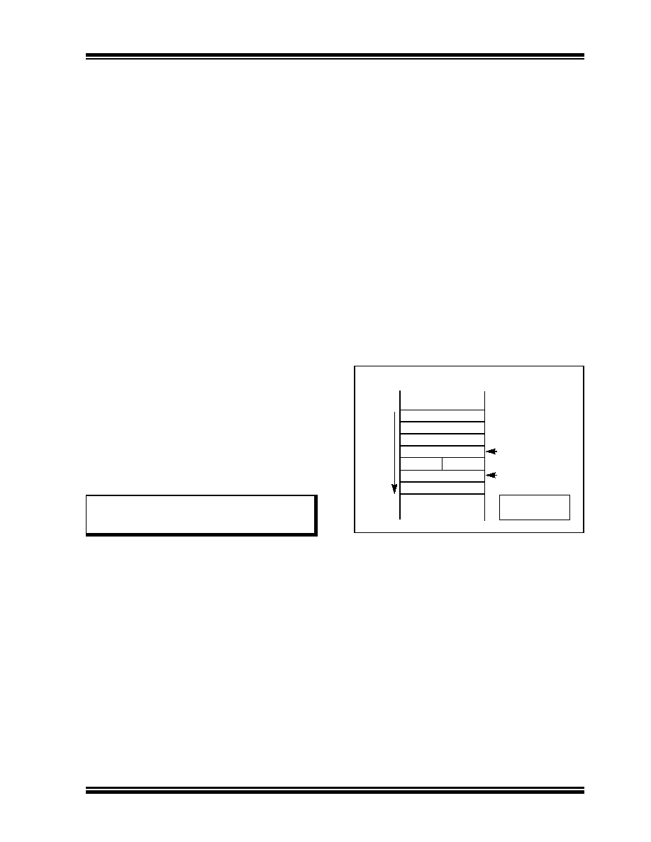
FIGURE 3-9:
CALL
STACK FRAME
Note:
A PC push during exception processing
will concatenate the SRL register to the
MSB of the PC prior to the push.
<Free Word>
PC<15:0>
000000000
0
15
W15 (before CALL)
W15 (after CALL)
S
tac
k
Gro
w
s
T
o
wa
rd
s
Hi
ghe
rAd
dr
es
s
PUSH
: [W15++]
POP
: [--W15]
0x0000
PC<22:16>
发布紧急采购,3分钟左右您将得到回复。
相关PDF资料
21FMN-BMTTR-A-TB
CONN FMN HSNG 21POS STAG REV SMD
PIC16LF87-I/ML
IC MCU FLASH 4KX14 EEPROM 28QFN
PIC24HJ32GP204-I/PT
IC PIC MCU FLASH 32K 44TQFP
20FMN-BMTTR-A-TB
CONN FMN HSNG 20POS STAG REV SMD
PIC16F88-I/SS
IC MCU FLASH 4KX14 EEPROM 20SSOP
18FMN-BMTTR-A-TB
CONN FMN HSNG 18POS STAG REV SMD
17FMN-BMTTR-A-TB
CONN FMN HSNG 17POS STAG REV SMD
PIC18LF46J11-I/ML
IC PIC MCU FLASH 64K 2V 44-QFN
相关代理商/技术参数
PIC18F4450T-I/ML
功能描述:8位微控制器 -MCU 16KB FL 768 RAM 34 I/O FS-USB 2.0 RoHS:否 制造商:Silicon Labs 核心:8051 处理器系列:C8051F39x 数据总线宽度:8 bit 最大时钟频率:50 MHz 程序存储器大小:16 KB 数据 RAM 大小:1 KB 片上 ADC:Yes 工作电源电压:1.8 V to 3.6 V 工作温度范围:- 40 C to + 105 C 封装 / 箱体:QFN-20 安装风格:SMD/SMT
PIC18F4450T-I/PT
功能描述:8位微控制器 -MCU 16KB FL 768 RAM 34 I/O FS-USB 2.0 RoHS:否 制造商:Silicon Labs 核心:8051 处理器系列:C8051F39x 数据总线宽度:8 bit 最大时钟频率:50 MHz 程序存储器大小:16 KB 数据 RAM 大小:1 KB 片上 ADC:Yes 工作电源电压:1.8 V to 3.6 V 工作温度范围:- 40 C to + 105 C 封装 / 箱体:QFN-20 安装风格:SMD/SMT
PIC18F4455-BL
制造商:POWERLITE SYSTEMS 功能描述:PIC18F445 W/ BOOTLOADER FOR FLASHLAB 制造商:POWERLITE SYSTEMS 功能描述:PIC18F445 W/ BOOTLOADER, FOR FLASHLAB 制造商:POWERLITE SYSTEMS 功能描述:PIC18F445 W/ BOOTLOADER, FOR FLASHLAB; Silicon Manufacturer:Powerlite Systems; Core Architecture:PIC; Kit Contents:Board; Features:Bootloader Programming, RS232 Connector for Boot-Loading and Serial Comms ;RoHS Compliant: Yes
PIC18F4455-I/ML
功能描述:8位微控制器 -MCU 24kBF 2048RM FSUSB2 RoHS:否 制造商:Silicon Labs 核心:8051 处理器系列:C8051F39x 数据总线宽度:8 bit 最大时钟频率:50 MHz 程序存储器大小:16 KB 数据 RAM 大小:1 KB 片上 ADC:Yes 工作电源电压:1.8 V to 3.6 V 工作温度范围:- 40 C to + 105 C 封装 / 箱体:QFN-20 安装风格:SMD/SMT
PIC18F4455-I/P
功能描述:8位微控制器 -MCU 24kBF 2048RM FSUSB2 RoHS:否 制造商:Silicon Labs 核心:8051 处理器系列:C8051F39x 数据总线宽度:8 bit 最大时钟频率:50 MHz 程序存储器大小:16 KB 数据 RAM 大小:1 KB 片上 ADC:Yes 工作电源电压:1.8 V to 3.6 V 工作温度范围:- 40 C to + 105 C 封装 / 箱体:QFN-20 安装风格:SMD/SMT
PIC18F4455-I/PT
功能描述:8位微控制器 -MCU 24kBF 2048RM FSUSB2 RoHS:否 制造商:Silicon Labs 核心:8051 处理器系列:C8051F39x 数据总线宽度:8 bit 最大时钟频率:50 MHz 程序存储器大小:16 KB 数据 RAM 大小:1 KB 片上 ADC:Yes 工作电源电压:1.8 V to 3.6 V 工作温度范围:- 40 C to + 105 C 封装 / 箱体:QFN-20 安装风格:SMD/SMT
PIC18F4455T-I/ML
功能描述:8位微控制器 -MCU 24kBF 2048RM FSUSB2 RoHS:否 制造商:Silicon Labs 核心:8051 处理器系列:C8051F39x 数据总线宽度:8 bit 最大时钟频率:50 MHz 程序存储器大小:16 KB 数据 RAM 大小:1 KB 片上 ADC:Yes 工作电源电压:1.8 V to 3.6 V 工作温度范围:- 40 C to + 105 C 封装 / 箱体:QFN-20 安装风格:SMD/SMT
PIC18F4455T-I/PT
功能描述:8位微控制器 -MCU 24kBF 2048RM FSUSB2 RoHS:否 制造商:Silicon Labs 核心:8051 处理器系列:C8051F39x 数据总线宽度:8 bit 最大时钟频率:50 MHz 程序存储器大小:16 KB 数据 RAM 大小:1 KB 片上 ADC:Yes 工作电源电压:1.8 V to 3.6 V 工作温度范围:- 40 C to + 105 C 封装 / 箱体:QFN-20 安装风格:SMD/SMT